
How to prevent thermal hotspots in an automotive power PCB
DETAILS
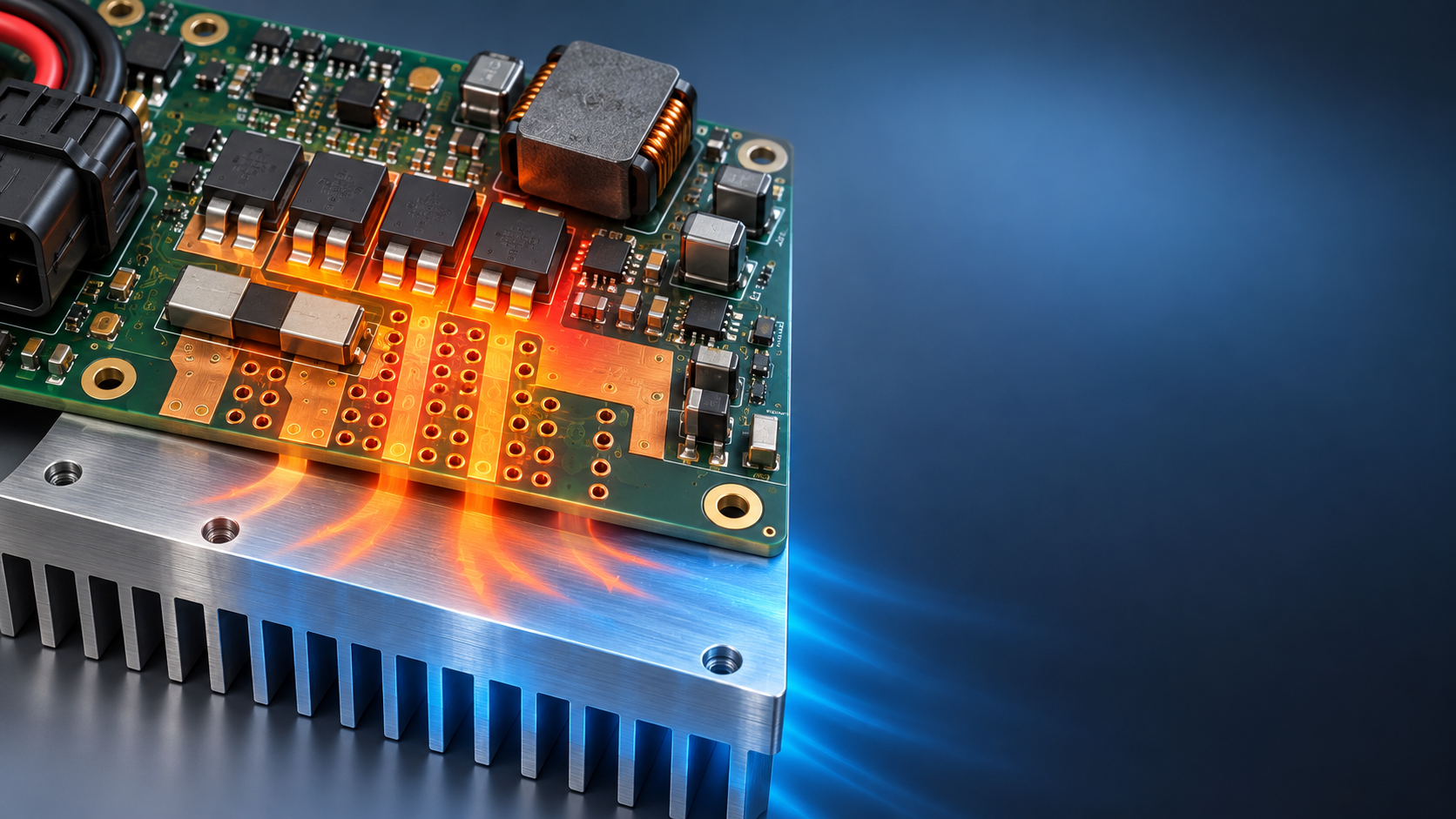
A thermal hotspot in an automotive power PCB is rarely caused by one undersized copper feature. It is usually the visible result of a thermal path that was treated as a layout detail rather than as part of the power-stage design. Heat generated in a MOSFET, gate driver, shunt, inductor, connector, or reverse-battery protection device must cross several interfaces before it reaches ambient air: the component package, solder joints, copper planes, plated vias, dielectric layers, mechanical housing, and sometimes a chassis-mounted heat sink.
If any link in that path has excessive thermal resistance, local temperature rises quickly even when the board’s average temperature appears acceptable. In an automotive power PCB, the consequence is not limited to reduced electrical efficiency. Localized heating can accelerate solder fatigue, increase MOSFET on-resistance, shift current sharing between parallel devices, degrade laminate and interface materials, and reduce margin during high-ambient or low-airflow operation.
The practical objective is therefore not simply to achieve the largest possible copper area. It is to control peak junction and board temperatures under the full electrical, mechanical, and environmental duty cycle, while ensuring that the fabrication and assembly process can repeatedly produce the intended thermal structure.
Start with the heat source, not the copper pour
Thermal mitigation begins with a credible loss model. A power transistor may dissipate heat through conduction loss, switching loss, body-diode loss, and transient stress. A shunt resistor produces I²R loss. Inductors combine winding loss with core loss, and connectors can create heat through contact resistance that may not be represented in a nominal schematic calculation. The design review should identify which losses dominate in each operating state rather than relying on one peak-power number.
For switching devices, conduction loss and switching loss often peak under different conditions. A MOSFET that remains cool at maximum load in steady conduction may become the primary hotspot during frequent switching transitions, regenerative operation, cold-crank conditions, or a high-bus-voltage event. Similarly, a DC/DC converter may show its highest thermal stress not at rated output power, but at an intermediate load where switching frequency, discontinuous conduction behavior, or control losses are unfavorable.
The relevant thermal condition must include more than ambient temperature. Evaluations should account for:
- maximum and minimum supply voltage, including operating transients where applicable;
- continuous current, overload current, inrush, and repetitive pulse loading;
- switching frequency, duty cycle, and operating mode;
- enclosure temperature and available airflow;
- nearby heat sources, such as motors, battery modules, or other control units;
- the expected duration of high-power operation rather than only instantaneous peaks.
A transient thermal analysis is especially important where the electrical load consists of short pulses. A board can tolerate a high loss for a short interval if the thermal mass and heat path are sufficient, but repeated pulses may establish a much higher equilibrium temperature than a single-pulse test suggests. Component transient thermal impedance curves are useful only when the test boundary conditions resemble the assembled product; a package mounted on a qualification board is not thermally equivalent to the final automotive PCB and housing.
Current density and thermal density are related, but not identical
High current density raises copper loss, but a low-resistance trace can still sit beside a severe hotspot created by a semiconductor package. The layout review needs to distinguish between heat generated in the copper and heat injected into the copper from components.
Power traces, planes, and pours should be sized using anticipated RMS current, temperature rise limits, copper thickness after plating, and the actual current path through neck-downs, vias, pads, fuses, and connectors. A wide pour is not useful if current is forced through a narrow connection between a pad and plane, or through a small cluster of vias at a layer transition. These localized restrictions create both electrical and thermal bottlenecks.
IPC-2152 offers a recognized basis for considering current-carrying conductor temperature rise, but it should not be treated as a substitute for product-specific simulation or validation. Its usefulness lies in establishing a disciplined starting point: conductor geometry, external versus internal layer placement, copper thickness, and neighboring copper all influence temperature rise. In a power board, the conductor is also a heat spreader, so its geometry must be assessed together with the semiconductor thermal footprint.
Thermal density is often more important than total board area. A compact cluster containing a high-side switch, low-side switch, current sense resistor, gate-driver supply network, and output inductor can produce mutually reinforcing heating. Spreading these elements without regard to switching-loop inductance is not a solution, but placing every loss-generating part into the smallest possible region can make a stable thermal design impossible. The layout must preserve electrical loop control while avoiding a concentrated thermal island.
Component placement determines whether heat can escape
The dominant power devices should be located where their primary heat path is usable. For a bottom-terminated MOSFET or power IC, that commonly means uninterrupted copper beneath the exposed pad, access to internal and opposite-side planes through thermal vias, and proximity to the mechanical surface intended to reject heat. Placing such a device near a board edge may help only if the edge connects effectively to a heat sink or conductive enclosure; otherwise, the reduced available copper can worsen the hotspot.
Heat-sensitive components deserve separation from power dissipation zones. Electrolytic capacitors, certain polymer capacitors, precision references, oscillators, sensors, and plastic connector bodies may have temperature limits or lifetime sensitivities that differ substantially from those of the power semiconductor. A component can meet its own electrical rating and still become the reliability-limiting element because it is exposed to sustained radiant and conducted heat from a nearby switch or inductor.
Placement should also consider assembly orientation and heat flow after installation. A board that is tested horizontally in still air may operate vertically in a sealed module, clamped to a metal base, or surrounded by harnesses that restrict convection. Where a housing is part of the thermal design, its contact pressure, flatness, coating, interface material, and mounting sequence become design variables, not mechanical afterthoughts.
Use vias as a designed thermal network
Thermal vias are effective when they connect a heat source to copper that can actually dissipate or redistribute heat. They are less effective when they merely transfer heat into a buried layer with no meaningful route to a larger plane, mounting surface, or enclosure.
Via design involves a trade-off among thermal conductance, electrical current capacity, manufacturability, solder behavior, and inspection requirements. A dense via array below an exposed pad can reduce vertical thermal resistance, but open vias may wick solder during reflow and leave insufficient solder under the package. Filled and capped vias can address this risk, though they add fabrication complexity and require clear specifications for filling, planarization, and cap quality. Tented vias may be appropriate in some locations but should not be assumed equivalent to filled vias under a thermal pad.
Via placement must also avoid weakening the solder-joint structure. Large void-prone pad geometries, uneven copper distribution, or poorly controlled via-in-pad construction can compromise the same interface intended to remove heat. The thermal performance of a package is highly dependent on the solder layer beneath it; a layout that looks thermally generous in CAD can underperform if assembly produces poor wetting, excessive voiding, or nonuniform standoff.
For high-current layer changes, the via network should be evaluated electrically as well as thermally. The relevant question is not whether one via meets a nominal ampacity estimate, but whether the complete via field shares current under real plane geometry. Uneven current entry, thermal relief patterns, and asymmetric pad connections can force disproportionate current through only part of the array.
Dielectric thickness and material selection affect vertical heat flow
Internal copper planes are valuable heat spreaders, but heat must cross the dielectric between layers. The thermal conductivity and thickness of the laminate therefore matter, particularly beneath bottom-cooled packages and in multilayer high-current regions. A stack-up optimized only for impedance, layer count, and cost may leave too much thermal resistance between the top-side power device and the lower-side heat-rejection surface.
Thinner dielectric layers can improve vertical conduction to adjacent planes, while thermally enhanced laminate systems may provide additional benefit in selected designs. Neither measure is automatically beneficial. Stack-up changes affect impedance control, dielectric breakdown margin, resin content, drill aspect ratio, copper balancing, warpage risk, and fabrication availability. Material data should also be reviewed under relevant operating conditions rather than treated as a single room-temperature value.
For automotive applications, the laminate choice must be compatible with expected temperature cycling, humidity exposure, voltage stress, and assembly profile. A low thermal resistance path is not sufficient if repeated expansion mismatch between copper, laminate, solder, and package creates fatigue or delamination risk. Environmental qualification frameworks such as ISO 16750 define vehicle-level environmental considerations, but the applicable OEM, module, and component requirements determine the actual acceptance conditions for a specific assembly.
Do not confuse copper area with usable heat sinking
A large copper pour removes heat efficiently only when it has a meaningful temperature gradient to a cooler region. Copper trapped around a hot device, bounded by other heat-generating components and insulated from the enclosure, may equalize temperature locally without lowering the peak enough. This is still useful for reducing gradients and improving solder-joint reliability, but it is not the same as rejecting heat from the module.
Effective heat sinking typically requires one or more of the following paths:
- conduction through copper and vias to a chassis-facing board surface;
- a direct thermal interface to a metal housing or heat spreader;
- an attached heat sink with controlled mounting pressure;
- airflow across surfaces that have enough exposed area to exchange heat;
- heat transfer through a dedicated substrate or insulated metal structure where the electrical architecture permits it.
Each interface adds resistance. Thermal interface materials can fill microscopic gaps, but excessive thickness, poor compression, pump-out during temperature cycling, or incomplete coverage can erase expected gains. The mechanical stack should define target compression and tolerance behavior. A thermal pad selected from a catalog conductivity value alone is not enough; its in-assembly bond-line thickness and contact conditions are usually more decisive.
Electrical layout errors can create thermal failures
Some hotspots originate from electrical parasitics rather than insufficient cooling. Excessive switching-loop inductance can increase ringing and switching loss. Poor gate-drive routing can slow transitions or create false turn-on, causing unexpected dissipation. Inaccurate current-sense routing can alter control behavior and push the converter into an inefficient operating mode. A high-current return path passing through shared copper can elevate local voltage and disturb control references.
This is why thermal and electrical reviews should use the same current-path map. The high di/dt loop should remain compact, but its copper should not be thermally isolated. Gate-driver decoupling must be placed for electrical performance without blocking heat spreading from the switching devices. Kelvin connections for current sensing and power-ground partitioning should be maintained without introducing narrow, resistive return paths.
Parallel MOSFETs require particular care. Devices with nominally similar part numbers do not necessarily share current equally once layout resistance, source inductance, gate resistance, package variation, and temperature coefficient are included. A warmer device can experience changing resistance and switching behavior, moving the thermal balance further away from the intended distribution. Symmetrical placement and matched copper paths are not cosmetic requirements; they are part of current-sharing control.
Validate the assembled board, not only the simulation model
Thermal simulation is valuable for comparing layouts and identifying likely bottlenecks, but its result depends on boundary conditions: material properties, copper distribution, interface assumptions, airflow, emissivity, enclosure coupling, and power dissipation estimates. The model should be correlated with physical measurements before it becomes the basis for a tight reliability margin.
Thermocouples, RTDs, and infrared imaging serve different purposes. Contact sensors provide repeatable point measurements when bonded correctly, but their placement can be difficult on small packages. Infrared imaging reveals gradients and unexpected hotspots rapidly, yet requires attention to surface emissivity, reflections, viewing angle, and calibration. A shiny copper area can appear cooler or hotter than its actual temperature if emissivity is not controlled.
Testing should include stabilized operation, transient loading, worst-case input voltage, realistic enclosure conditions, and the relevant ambient extremes. It should also examine temperature differences across parallel devices, connector pins, inductors, and thermal interface regions. A useful result is not simply a peak temperature value; it is an explanation of where the heat originates, how it moves through the assembly, and which margin remains after component tolerances and manufacturing variation are considered.
Manufacturing controls are part of hotspot prevention
Power PCB thermal performance can be undermined by ordinary production variation. Final copper thickness, via plating quality, registration, solder-mask-defined pad behavior, solder-paste deposition, reflow profile, and voiding beneath thermal pads all affect heat transfer. Fabrication documentation should specify the features that are thermally critical rather than leaving them implied by artwork alone.
For multilayer boards, the stack-up should identify finished copper requirements, dielectric thicknesses in critical regions, and any controlled via structure. For assembly, the thermal-pad stencil design, paste type, reflow window, and inspection approach should be aligned with the package supplier’s recommendations and the module’s acceptance criteria. IPC workmanship and performance standards can provide a common vocabulary, but they do not replace a product-specific thermal acceptance plan.
The most reliable automotive power PCB is not the board with the maximum amount of copper. It is the board in which loss generation, current flow, heat spreading, vertical conduction, mechanical interfaces, and production capability have been evaluated as one system. When a hotspot appears late in development, the correct response is to trace that complete system path. Enlarging a copper pour may help, but it should be the conclusion of that analysis—not the default remedy.
Recommended News
- Heat DissipationHow to prevent overheating in automotive PCB power distributionPrevent overheating in automotive PCB power distribution with practical tips on copper layout, thermal paths, and testing. Discover how to reduce hotspots and improve reliability.
- Heat DissipationCan heat spreading intelligence identify hot spots in PCB designs?Discover how heat spreading intelligence identifies PCB hot spots before fabrication. Learn to assess thermal models, validate predictions, and choose design changes that improve reliability.
- Heat DissipationWhich heat sink materials suit high-power electronics made in Germany?Heat sink materials Germany: compare aluminum, copper, graphite, and hybrid designs for high-power electronics. Find the right balance of thermal performance, weight, cost, and manufacturability.
- Heat DissipationHow to assess a graphite materials supplier's capability for thermal partsGraphite materials supplier assessment starts with more than machining. Discover how to evaluate thermal performance, purity, precision, cleanliness, traceability, and testing for reliable thermal parts.
- Heat DissipationHow to assess a heat dissipation supplier before placing an orderHeat dissipation supplier assessment guide: verify thermal performance, materials, process control, samples, capacity, and total risk before placing an order.
- Heat DissipationHow automotive PCB material selection affects thermal reliabilityAutomotive PCB material selection shapes thermal reliability. Explore CTE, Tg, moisture resistance, stack-up design, and proven qualification strategies for demanding vehicle electronics.