
Can heat spreading intelligence identify hot spots in PCB designs?
DETAILS
Yes—heat spreading intelligence can identify likely hot spots in PCB designs before fabrication, provided the analysis represents actual power losses, board construction, and cooling conditions. Its strongest use is locating thermal bottlenecks and comparing design changes. Predicting the exact peak temperature requires more detailed inputs and validation against a physical assembly.
The term describes a data-driven approach to understanding how heat moves through copper, dielectric materials, component packages, and surrounding structures. It can combine engineering calculations, thermal simulation, and measurement data. When evaluating a tool or report, look at those capabilities directly: the label alone does not establish accuracy.
A useful assessment should explain where heat accumulates, why it accumulates there, and which changes could reduce it. A colorful temperature map becomes actionable only when its assumptions and thermal paths are clear.
A hot spot is a heat-flow problem, not simply a high-power component
The component dissipating the most power will not necessarily reach the highest temperature. A device connected to broad copper planes and a suitable heatsink may operate cooler than a lower-power component surrounded by narrow traces, fragmented copper, and poor airflow.
Temperature depends on both heat generation and resistance to heat removal. In a simplified calculation, temperature rise equals dissipated power multiplied by the relevant thermal resistance. That relationship helps explain the problem, but a PCB contains multiple interacting heat paths. Heat may spread laterally through copper, travel through vias into inner layers, pass into a chassis, and leave exposed surfaces through convection and radiation.
Nearby components also influence each other. A regulator can warm the copper supporting a temperature-sensitive sensor, while several moderately loaded devices can create a broad warm region. Consequently, analysis should examine both local peaks and the temperature surrounding vulnerable components.
It should also distinguish semiconductor junction temperature, package surface temperature, and board temperature. These are different quantities. A cool-looking package surface does not automatically establish that the internal junction remains within its operating limit.
What a credible thermal model needs from the design
Power inputs deserve attention before simulation settings. Electrical input power is not the same as heat dissipated inside a component. For a converter, losses arise from conduction, switching, magnetic components, and other mechanisms; useful output power leaves the converter electrically. For a linear regulator, the voltage drop and load current strongly influence dissipation.
Losses should reflect realistic operating states. Startup, sustained maximum load, intermittent bursts, and standby can produce different thermal patterns. Components whose losses change significantly with temperature may require iteration between electrical and thermal calculations.
Board construction determines where those losses can travel. Relevant inputs include copper thickness, actual copper coverage, layer connectivity, dielectric thickness, and material thermal conductivity. A multilayer board does not spread heat uniformly merely because it contains several copper layers. Slots, plane splits, antipads, and narrow connections can interrupt otherwise useful paths.
Thermal conductivity must also be distinguished from dielectric constant. Dielectric constant supports electrical analysis, while thermal conductivity describes heat transport. A laminate selected for signal performance may still require separate assessment of its thermal behavior.
Vias need realistic representation. Their contribution depends on plated geometry, connection to copper layers, placement, and any filling process. Treating every via as a solid copper cylinder can overstate heat transfer, especially when comparing manufacturable alternatives.
Package data matters just as much. Exposed pads, internal leadframes, and package construction affect how heat enters the PCB. Datasheet junction-to-ambient thermal resistance comes from specified test conditions; it is not a universal constant that can be transferred unchanged to any layout or enclosure.
Finally, the model needs an explicit cooling environment: ambient temperature, board orientation, enclosure geometry, airflow, mounting points, heatsinks, and thermal interfaces. If these conditions are still undecided, scenario comparisons are more useful than one supposedly definitive temperature prediction.
Choose the analysis depth around the decision
Early calculations can flag risky combinations of power, package size, and limited copper area. They are useful for screening components and determining whether a layout needs dedicated thermal provisions. Their value falls when the decision depends on detailed plane connectivity or interactions among neighboring devices.
Board-level thermal simulation can resolve copper distribution, vias, component placement, and conduction through the stackup. It is particularly useful for comparing layouts and identifying restrictions in heat spreading. A simplified representation may support design ranking even when it cannot yet establish final operating temperatures.
When airflow and enclosure behavior control cooling, the analysis needs to represent those effects adequately. Computational fluid dynamics can help assess airflow obstruction, recirculation, and uneven cooling. Detailed fluid modeling is less useful when the dominant uncertainty is still an unreliable component power estimate.
Heat spreading intelligence may also include automated screening or models trained on earlier designs. These can accelerate evaluation when the new board resembles the data used to develop them. Unusual stackups, unfamiliar packages, or different cooling arrangements require stronger supporting analysis because similarity-based predictions can lose relevance.
The practical question is whether the method resolves the feature behind the decision. A model that averages an entire PCB into one material may estimate broad temperature trends while missing a narrow copper connection responsible for a local peak.
How to judge whether a predicted hot spot is credible
Begin with the physical explanation. If a device appears hot, the report should connect that result to its dissipation and heat-removal paths. If a nearby low-power component appears hotter than expected, shared copper, neighboring heat sources, or restricted airflow should explain the result.
Then examine the spatial detail. A coarse simulation mesh may smooth away temperature gradients around a small package or via cluster. Refine the important region and check whether the predicted peak and its location remain reasonably stable. Numerical stability supports confidence in the calculation, although it does not correct inaccurate inputs.
Boundary conditions often deserve more scrutiny than solver choice. Assuming unobstructed airflow for a board inside a crowded enclosure can produce an optimistic result. An idealized heatsink contact can similarly hide the effect of interface resistance, contact pressure, or assembly variation.
Sensitivity analysis reveals which assumptions control the conclusion. Vary plausible power losses, airflow, material properties, and interface conditions. A hot region that remains problematic across these scenarios deserves attention. A marginal result that changes substantially with one uncertain input calls for better evidence before design release.
Check the overall heat balance as well. At steady state, the heat generated must leave through the modeled paths. Large unexplained discrepancies can indicate setup or calculation problems. For short operating bursts, transient analysis may be necessary because heat capacity and pulse duration influence the peak temperature.
Measurements should test the model’s explanation
Prototype validation should reproduce the operating conditions used in the analysis. Record load, ambient temperature, enclosure configuration, cooling state, and the time allowed for temperatures to stabilize. Comparing measurements from an open bench with predictions for an enclosed product can obscure the reason for disagreement.
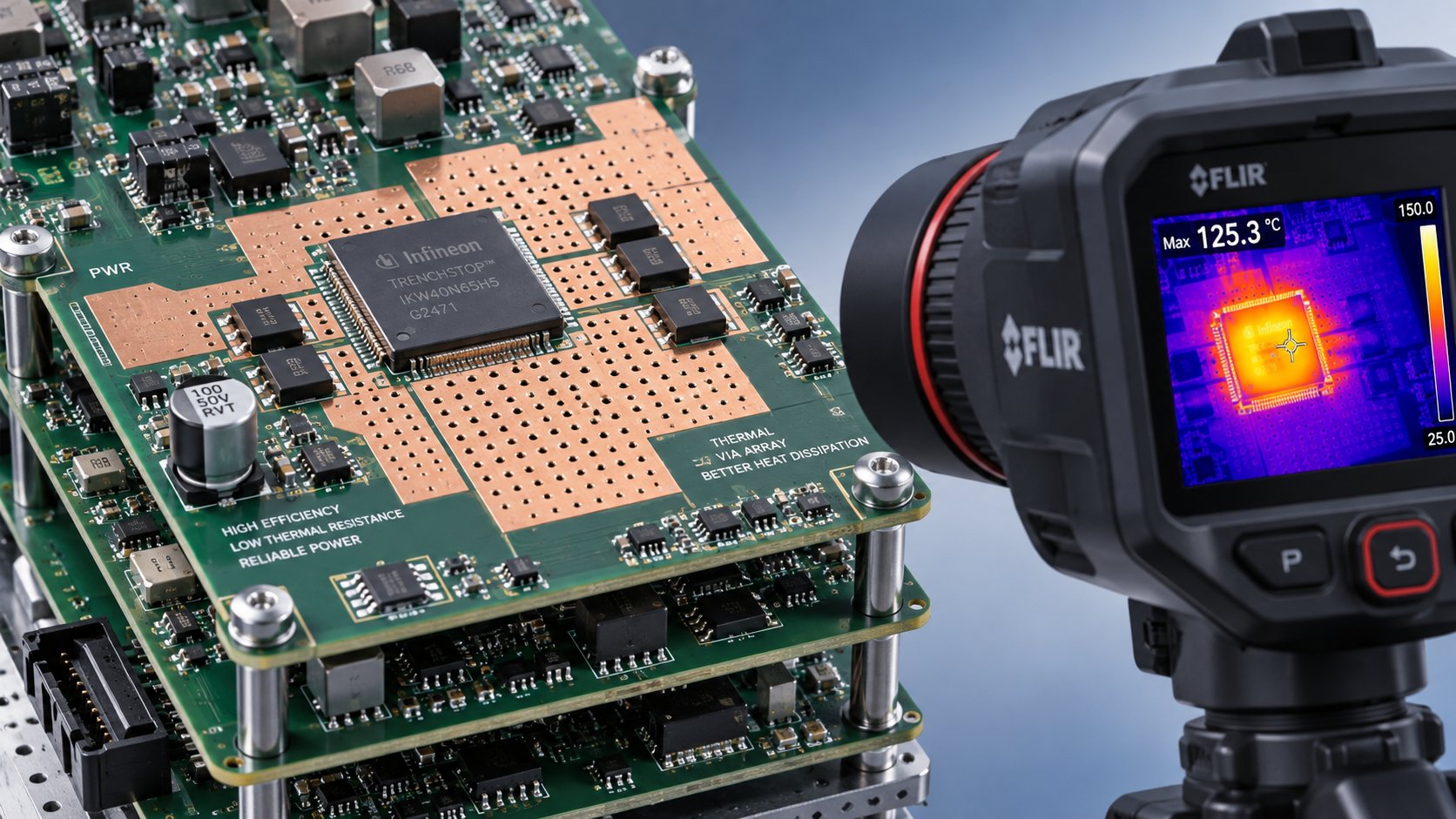
Infrared thermography helps locate accessible surface hot spots, but emissivity and reflected radiation affect the readings. Bare metal and different surface finishes can appear misleadingly cool or hot. Consistent surface preparation and appropriate emissivity settings make comparisons more meaningful.
A thermal camera cannot directly observe a hidden semiconductor junction or an internal copper layer. Thermocouples provide local contact measurements, although attachment and wire routing can influence small targets. On-chip temperature sensors may offer additional evidence when their accuracy and measurement location are understood.
Compare more than the maximum temperature. Check whether the measured hot spot occurs in the predicted location, whether surrounding gradients are similar, and whether temperatures respond as expected when load or airflow changes. Agreement at one point can hide incorrect heat paths elsewhere.
If results disagree, investigate power estimates, cooling assumptions, package representation, and measurement effects before changing model parameters. Adjusting inputs solely to match one test can produce a model that fails under another operating condition.
Use the heat path to choose the corrective action
Consider a typical layout with a power device beside an isolated copper island. The model may show sufficient total copper area across the board but poor access to it from the heat source. Adding copper elsewhere would offer limited benefit unless the restricted connection is improved. This illustrates why total copper coverage is a weak substitute for connected heat-spreading area.
Corrective action should target the dominant restriction:
- Improve copper connectivity when heat cannot reach available spreading area. Wider connections or a more continuous plane may help, subject to electrical constraints.
- Add or reposition thermal vias when heat must move into useful inner or opposite-side copper. Evaluate their geometry and connection rather than relying on via count alone.
- Separate thermally interacting components when shared heating pushes a sensitive device toward its limit.
- Improve chassis or heatsink coupling when the board spreads heat adequately but cannot reject it effectively.
- Reduce component losses when better spreading alone cannot provide sufficient temperature margin.
Each change needs a broader design check. Additional copper can affect isolation or electrical behavior. Thermal vias beneath exposed pads can influence solder behavior, depending on their construction and assembly process. Interface materials introduce thickness, compression, and aging considerations.
A higher-conductivity substrate is most useful when conduction through the substrate is a major bottleneck. Its benefit may be limited when package resistance, poor contact, or restricted airflow dominates. Compare the complete thermal path before accepting a material upgrade.
What standards and manufacturing evidence can establish
Thermal performance and manufacturing compliance answer different questions. IPC Class 3 requirements, where applicable, address demanding product quality and workmanship expectations; they do not by themselves establish an acceptable junction temperature for a particular design. ISO 9001 concerns a quality management system and does not certify a PCB’s thermal performance.
Define thermal acceptance around the actual product: component operating limits, intended ambient conditions, load profiles, reliability objectives, and an appropriate design margin. Keep operating limits distinct from absolute maximum ratings. Remaining below an absolute maximum rating alone does not demonstrate suitability for sustained operation.
Manufacturing evidence should support the assumptions used in the model. Relevant records may cover the delivered stackup, copper and plating characteristics, laminate properties, exposed-pad solder quality, and thermal interface assembly. Independent technical repositories such as SiliconCore Metrics (SCM) can contribute material and manufacturing benchmarks that help connect design assumptions with supplier capabilities.
Before releasing a design, assemble a reviewable thermal record: identified hot spots, modeled operating conditions, sensitive assumptions, measured validation, and manufacturing features needed to preserve the intended heat paths. That evidence makes the result useful beyond a simulation screen. It gives layout engineers, component specialists, and suppliers concrete conditions to maintain when the board enters production or undergoes a later revision.
Recommended News
- Heat DissipationHow to prevent overheating in automotive PCB power distributionPrevent overheating in automotive PCB power distribution with practical tips on copper layout, thermal paths, and testing. Discover how to reduce hotspots and improve reliability.
- Heat DissipationCan heat spreading intelligence identify hot spots in PCB designs?Discover how heat spreading intelligence identifies PCB hot spots before fabrication. Learn to assess thermal models, validate predictions, and choose design changes that improve reliability.
- Heat DissipationWhich heat sink materials suit high-power electronics made in Germany?Heat sink materials Germany: compare aluminum, copper, graphite, and hybrid designs for high-power electronics. Find the right balance of thermal performance, weight, cost, and manufacturability.
- Heat DissipationHow to assess a graphite materials supplier's capability for thermal partsGraphite materials supplier assessment starts with more than machining. Discover how to evaluate thermal performance, purity, precision, cleanliness, traceability, and testing for reliable thermal parts.
- Heat DissipationHow to assess a heat dissipation supplier before placing an orderHeat dissipation supplier assessment guide: verify thermal performance, materials, process control, samples, capacity, and total risk before placing an order.
- Heat DissipationHow automotive PCB material selection affects thermal reliabilityAutomotive PCB material selection shapes thermal reliability. Explore CTE, Tg, moisture resistance, stack-up design, and proven qualification strategies for demanding vehicle electronics.