
Multi layer PCB design guide for controlling signal crosstalk
DETAILS
Controlling Crosstalk in Multi-Layer PCB Design
A robust multi layer PCB design guide begins with controlling signal crosstalk before it compromises timing margins, data integrity, or EMC performance.
For technical evaluators, stackup selection, reference-plane continuity, dielectric properties, trace spacing, and return-path design must be assessed as measurable engineering variables.
This guide outlines practical, data-driven methods for reducing coupling in high-density multilayer boards while supporting reliable IPC-Class 3-level performance.
What Technical Evaluators Need to Confirm First
The central search intent behind a multi layer PCB design guide is not simply learning routing terminology. Evaluators need confidence that a proposed board can meet electrical requirements before production.
Crosstalk becomes critical when fast edge rates, dense routing channels, high layer counts, and mixed signal interfaces reduce the available design margin.
The first engineering question is whether the design team has identified aggressive nets based on rise time, routing length, impedance sensitivity, and receiver threshold.
A relatively slow clock can create substantial coupling if its edge rate is fast, its trace is long, and its adjacent reference structure is weak.
Technical evaluators should therefore request a signal classification table rather than relying on broad labels such as high speed, low speed, digital, or analog.
That table should identify clocks, differential links, memory buses, switching nodes, reset signals, precision analog paths, and sensitive control interfaces separately.
The second question is whether the PCB fabricator can repeatedly build the assumed stackup. Simulation results have little value when actual dielectric thickness varies beyond tolerable limits.
Board approval should connect electrical rules to fabricator capability data, including laminate family, resin content, copper weight, press cycle, and controlled impedance tolerance.
Understand the Coupling Mechanisms Before Setting Rules
Crosstalk is unwanted energy transfer from an aggressor trace into a nearby victim trace. It appears as voltage noise, timing disturbance, false switching, or degraded eye opening.
Capacitive coupling occurs through the electric field between adjacent conductors. It becomes stronger as traces move closer together or as their parallel run length increases.
Inductive coupling occurs through the magnetic field generated by changing current. It depends heavily on loop area, return-path geometry, and signal current direction.
Near-end crosstalk is generally observed at the source side of the victim trace. Far-end crosstalk appears near the victim receiver after coupled energy propagates.
Microstrip and stripline routes do not behave identically. External microstrips expose more field energy to air, while internal striplines couple primarily through controlled dielectric structures.
Stripline routing between solid reference planes usually offers stronger field containment. However, poor plane spacing or excessively dense internal channels can still create meaningful coupling.
Differential pairs require separate analysis because pair members intentionally couple to each other. Their external spacing must prevent nearby aggressors from disrupting differential balance.
Switching regulator nodes deserve special attention because their fast voltage transitions can inject noise into nearby traces even when average switching frequency is modest.
Start With a Stackup That Supports Field Containment
The stackup is the most important crosstalk-control decision because it determines trace geometry, reference-plane distance, dielectric consistency, and available routing channels.
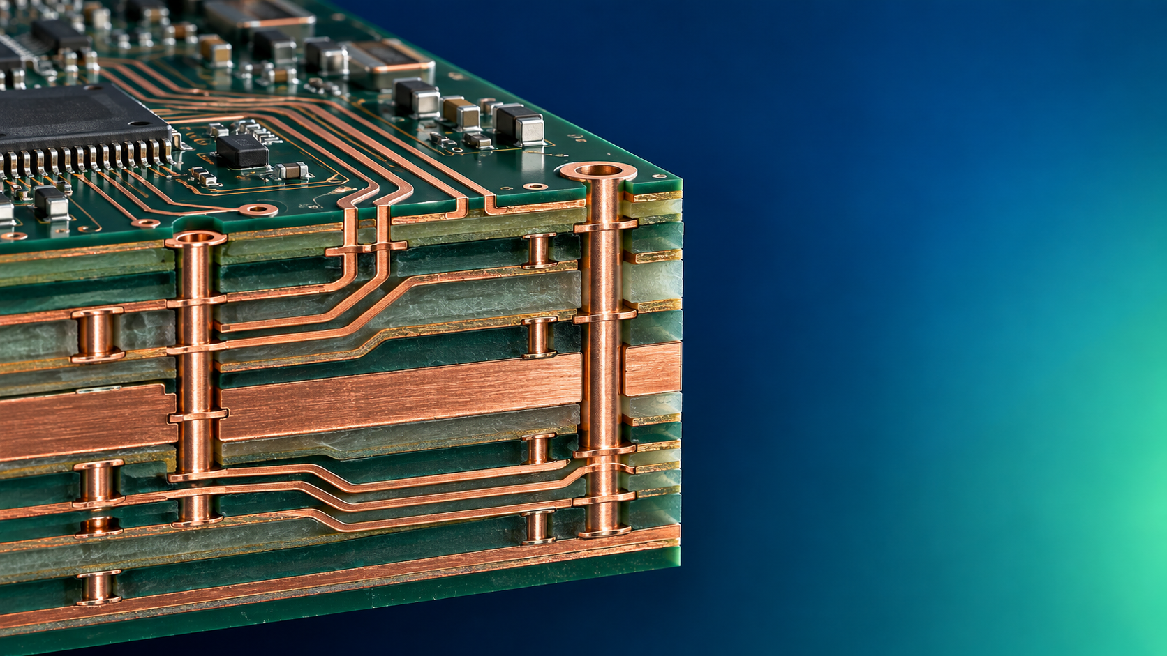
A practical multi layer PCB design guide should treat stackup definition as an electrical specification, not an administrative layer assignment completed after placement.
For sensitive single-ended signals, placing a routing layer directly adjacent to a continuous ground plane reduces loop area and constrains electromagnetic fields.
Thin dielectric spacing between a signal layer and its reference plane generally improves field containment. It also enables narrower traces for a target impedance.
However, very thin dielectric constructions can increase fabrication complexity, affect etching tolerances, and raise sensitivity to copper thickness variation across the panel.
Technical evaluators should compare the electrical advantage of tighter plane spacing against yield, material availability, and the fabricator's proven registration capability.
Adjacent routing layers should preferably run orthogonally when broad parallelism cannot be avoided. Orthogonal orientation reduces sustained side-by-side field interaction between layers.
Signal layers should not be placed directly adjacent without a practical reason. When this arrangement is unavoidable, routing direction and separation rules must become stricter.
Choose Dielectric Materials Using Measured Electrical Data
Material selection affects crosstalk because dielectric constant influences impedance, propagation delay, field distribution, and the physical geometry required for controlled routing.
Nominal dielectric constant values from laminate catalogs are useful starting points, but technical approval should consider the test method and frequency of each reported value.
Design calculations can drift when fabricators substitute materials with different resin content, glass weave style, or effective dielectric behavior at operating frequencies.
For high-speed digital interfaces, use the fabricator's actual stackup data whenever possible. This includes pressed dielectric thickness rather than only pre-preg nominal thickness.
Glass weave can also create local impedance variation and differential skew. This risk is especially relevant for long, tightly coupled differential pairs operating at high data rates.
Low-loss materials may improve insertion loss, but they do not automatically solve crosstalk. Spacing, return planes, routing topology, and discontinuity control remain necessary.
Evaluators should require documented dielectric constant and dissipation factor values tied to a specified frequency range, resin system, and finished board construction.
Material qualification should also include thermal reliability because delamination, resin degradation, and dimensional instability can alter electrical performance during long-term service.
Set Trace Spacing Rules Based on Geometry, Not Habit
Rules such as three times trace width or five times trace width are useful screening shortcuts, but they are not universal crosstalk guarantees.
The required separation depends on trace height above the reference plane, trace width, copper thickness, dielectric constant, signal amplitude, rise time, and parallel length.
A 3W rule may be inadequate when traces are far from their reference plane. Conversely, it can be overly conservative in tightly referenced stripline structures.
For external microstrip layers, spacing should be evaluated with electromagnetic field simulation when interfaces have tight timing budgets or strict emission limits.
Internal stripline layers often allow denser routing because their fields are more contained. Still, prolonged parallel routing can create unacceptable near-end coupling.
Long parallel runs matter more than brief crossings. A short orthogonal crossing between layers is usually less harmful than a long adjacent route on one layer.
Critical nets should receive dedicated keepout zones where possible. This is particularly valuable around clocks, high-speed serial transmitters, memory strobes, and analog references.
Spacing rules should distinguish ordinary digital nets from high-priority nets. One universal rule often wastes routing area while failing to protect the signals that matter most.
Protect Return Paths and Plane Continuity
Signal current always requires a return path. At high frequencies, that return current follows the path of lowest inductance, usually directly beneath the routed trace.
A continuous reference plane below or above the signal route minimizes loop area. It reduces inductive coupling while improving impedance consistency and radiated-emission behavior.
Splits, slots, voids, and poorly placed anti-pads force return current to detour. The enlarged loop can increase noise, mode conversion, and susceptibility to crosstalk.
A signal should not cross a plane split unless the return path has been deliberately engineered. This principle applies even to apparently low-speed control traces.
When a signal changes layers, nearby stitching vias can provide a low-inductance path for return current between associated reference planes.
Ground stitching becomes especially important when a signal transitions between layers referenced to different planes. Without it, return current may spread unpredictably through the board.
Power planes can serve as high-frequency references only when their impedance to ground is sufficiently low across the relevant frequency spectrum.
Technical reviewers should inspect plane shapes, via fields, connector transitions, and decoupling placement together. Return-path integrity is a system property rather than a routing detail.
Route Differential Pairs and Single-Ended Nets Differently
Differential routing reduces sensitivity to external noise when pair symmetry is maintained. It does not eliminate crosstalk caused by nearby signals or discontinuous reference structures.
Pair members should remain tightly coupled according to the impedance model. Excessive separation increases common-mode noise vulnerability and makes external coupling more likely.
At the same time, neighboring differential pairs require sufficient separation. Dense pair bundles can create pair-to-pair crosstalk and degrade common-mode rejection.
Maintain consistent pair geometry through bends, vias, connectors, and layer changes. Unequal discontinuities create skew and convert differential energy into common-mode energy.
Length matching should be applied only where timing analysis requires it. Unnecessary serpentine structures can add parallel segments, resonances, and extra coupling opportunities.
When delay tuning is necessary, use compact, well-spaced tuning patterns. Keep them away from clocks, connectors, switching nodes, and other sensitive routes.
Single-ended clock lines deserve dedicated routing treatment because their transitions can inject deterministic noise into nearby timing-critical victim nets.
Separate analog traces from digital aggressors by using routing layers, ground shielding, spatial distance, and controlled entry points rather than relying on labels alone.
Use Vias, Connectors, and Shields With Intent
Vias are often treated as simple interconnects, yet they can become significant discontinuities in high-speed boards. Their stubs, pads, and antipads affect impedance and coupling.
Long via stubs can resonate and degrade signal quality. Backdrilling or blind and buried vias may be justified when link speed and routing architecture demand it.
Via transitions should preserve the intended return path. Ground vias near signal vias reduce inductance and help contain fields during layer changes.
Connector pin assignments should avoid placing aggressive signals beside sensitive receivers whenever the interface definition allows alternate pin mapping.
Ground pins or ground vias between sensitive channels can reduce coupling substantially. Their value should be confirmed through simulation or measurement for the specific geometry.
Ground guard traces can help in selected cases, but they are not a substitute for proper plane reference and adequate spacing. Poorly stitched guards may offer limited benefit.
Guard traces require frequent grounding vias and enough room to avoid creating an uncontrolled routing channel. Their implementation must match the board's fabrication rules.
Metal shielding is appropriate when noise sources or victim circuits cannot be separated sufficiently through layout. It should be evaluated for cost, thermal impact, and assembly complexity.
Validate Crosstalk Through Simulation, Fabrication Data, and Test
Design rules are only assumptions until validated. The most defensible workflow combines field-solver analysis, stackup confirmation, prototype measurement, and production capability review.
Pre-layout simulations help establish trace width, spacing, layer assignment, and reference-plane requirements. Post-layout extraction identifies coupling introduced by actual routing constraints.
Simulation models must reflect realistic copper thickness, finished dielectric dimensions, solder mask effects, via structures, and connector behavior where relevant.
During prototype qualification, measure impedance and channel behavior using suitable methods such as TDR, vector network analysis, eye diagrams, or targeted oscilloscope probing.
Measurement should focus on representative worst-case channels rather than convenient test points. Include long parallel routes, layer transitions, dense connector regions, and power-interface boundaries.
Fabricator documentation should confirm actual controlled impedance results, coupon methodology, stackup release data, registration capability, and any material substitutions made before production.
For IPC-Class 3 applications, crosstalk review should sit alongside reliability assessment. Electrical margin can be lost when fabrication variation, thermal cycling, and assembly stress combine.
Independent benchmarking is useful when comparing manufacturing partners. It turns informal claims about high-speed capability into reviewable evidence tied to measurable process performance.
Create an Approval Checklist for High-Density Multilayer Boards
Before approving fabrication, technical evaluators should verify that every critical signal has a defined layer, impedance target, reference plane, spacing rule, and return-path strategy.
Confirm that the released stackup matches the exact laminate family and press construction intended for manufacturing. Generic material descriptions are insufficient for sensitive designs.
Review the longest parallel runs involving aggressive and victim nets. Prioritize clock lines, high-speed serial channels, memory interfaces, switching nodes, and precision analog paths.
Check every layer transition for return-via placement and reference-plane compatibility. A clean route on one layer can fail electrically at an uncontrolled transition.
Require evidence that design constraints are manufacturable at the selected supplier. This includes minimum spacing, drill tolerances, copper distribution, buildup capability, and impedance coupons.
Ask whether simulation assumptions were reconciled with fabrication data. Differences in dielectric thickness or copper profile should trigger a new review before release.
Finally, define acceptance criteria in measurable terms, such as impedance tolerance, maximum crosstalk level, eye-mask margin, insertion loss, and timing budget allocation.
A documented checklist enables consistent decisions across engineering, quality, sourcing, and supplier-management teams while reducing dependence on individual design intuition.
Conclusion
An effective multi layer PCB design guide for controlling signal crosstalk starts with stackup discipline, not isolated routing rules or generic spacing formulas.
Technical evaluators should assess field containment, dielectric consistency, reference continuity, parallel routing, via transitions, and measurable supplier capability as one connected system.
The strongest designs translate signal-integrity requirements into manufacturable constraints, then validate those constraints with realistic models, prototype data, and documented fabrication controls.
When these decisions are made early, dense multilayer boards can achieve stronger timing margin, lower noise risk, improved EMC performance, and more reliable IPC-Class 3 production outcomes.
Recommended News
- HDI TechnologyHow to vet PCB suppliers in a directory before requesting quotesPCB suppliers directory guide: learn how to verify capabilities, certifications, traceability, and quote assumptions before selecting a reliable PCB partner.
- HDI TechnologyHow UAE engineering data repositories improve design traceabilityEngineering data repository UAE solutions strengthen design traceability by linking requirements, revisions, supplier evidence, and manufacturing data. Explore practical ways to reduce risk and accelerate releases.
- HDI TechnologyHow to verify UL recognition for printed circuit boardsPrinted circuit boards UL verification made clear: learn how to check UL marks, file numbers, factory scope, stack-ups, and traceability for audit-ready compliance.
- HDI TechnologyMulti layer PCB design guide for controlling signal crosstalkMulti layer PCB design guide for controlling signal crosstalk with stackup, spacing, return-path, and validation strategies for reliable high-density boards.
- HDI TechnologyHow tighter manufacturing tolerances change HDI PCB pricesMicro tolerance manufacturing price explained: see how tighter HDI PCB tolerances affect yield, inspection, supplier options, and sourcing costs.
- HDI TechnologyHow automotive PCB impedance control prevents signal failuresAutomotive PCB impedance control prevents reflections, noise, and timing errors in ADAS, EV, and infotainment systems. Learn how to build reliable signal paths.