
How dielectric constant affects impedance stability in RF modules
DETAILS
How Dielectric Constant Affects Impedance Stability in RF Modules
For technical evaluators, dielectric constant is not merely a laminate datasheet value. It directly determines whether RF impedance remains stable across frequency, temperature, fabrication lots, and assembled module configurations.
The practical conclusion is straightforward: a nominal dielectric constant cannot qualify an RF material alone. Evaluators must examine variation, test method, frequency dependence, resin distribution, and stackup control together.
When these factors are not controlled, a theoretically correct transmission line can drift from its target impedance. That drift increases reflections, alters matching networks, and reduces manufacturing yield.
This article explains how the dielectric constant for RF modules affects impedance stability, which material properties deserve scrutiny, and how evaluators can benchmark suppliers before releasing production designs.
Why Dielectric Constant Drives RF Impedance Stability
Dielectric constant, commonly written as Dk or relative permittivity, describes how strongly a material stores electric energy compared with vacuum. It affects electromagnetic field propagation within PCB structures.
In RF modules, controlled impedance traces depend on the interaction between conductor geometry and the surrounding dielectric. Microstrip, stripline, grounded coplanar waveguide, and embedded lines respond differently.
For a given trace width and dielectric thickness, a higher dielectric constant generally produces lower characteristic impedance. A lower dielectric constant generally produces higher characteristic impedance.
This relationship matters because RF circuits are typically designed around fixed impedance targets. Common targets include 50 ohms for single-ended lines and 100 ohms for differential interfaces.
If actual Dk differs from the value used during field-solver modeling, the manufactured line no longer behaves as intended. Matching, filtering, antenna feed, and phase-sensitive functions may shift.
Impedance stability is therefore not equivalent to achieving one acceptable impedance measurement during qualification. It means maintaining consistent electrical behavior across material batches, panels, process conditions, and operating environments.
For technical evaluators, the key question is not simply whether a supplier advertises low Dk. The relevant question is whether its effective dielectric constant remains predictable in the intended construction.
Nominal Dk Is Less Important Than Effective Dk Control
Datasheets commonly list a nominal Dk value, but this value is measured under specific conditions. Those conditions may not represent the final RF module stackup or operating frequency.
Effective dielectric constant is the value experienced by the propagating RF field in a finished transmission structure. It depends on dielectric composition, trace geometry, copper profile, and nearby conductors.
In microstrip structures, part of the field propagates through air and part through the substrate. The effective Dk is therefore lower than the bulk dielectric constant.
Stripline structures confine more electromagnetic field within the dielectric. Their impedance and phase response are more directly influenced by the laminate Dk and prepreg resin distribution.
For high-density RF modules, field distribution can also be affected by solder mask, conformal coating, shielding cavities, bonding materials, and adjacent layers. Simplified calculations often miss these effects.
Evaluators should request the supplier’s stackup-specific impedance model rather than relying only on generic laminate tables. The model should identify Dk assumptions by layer type and frequency.
It is also important to distinguish between core material Dk and cured prepreg Dk. Their values can differ because prepreg resin flow changes glass-to-resin proportions after lamination.
When core and prepreg materials have inconsistent effective Dk values, traces on different layers can exhibit different impedance despite having nominally similar geometries. This creates hidden design asymmetry.
Frequency Dependence Can Shift Impedance Across the RF Band
Dielectric constant is not always constant across frequency. Many materials exhibit dispersion, meaning Dk changes as frequency increases. RF module behavior can therefore vary across the operating band.
A material characterized at one gigahertz may behave differently at six, twenty-eight, or seventy-seven gigahertz. This difference becomes increasingly important in wideband and millimeter-wave applications.
Frequency-dependent Dk changes both characteristic impedance and phase velocity. In narrowband circuits, the impact may be manageable. In broadband filters, phased arrays, and radar modules, it can become critical.
Phase delay is especially sensitive because it accumulates over trace length. Small Dk differences can create meaningful phase mismatch between channels, even when individual impedance readings appear acceptable.
Technical evaluators should request Dk data at frequencies relevant to the final product, not merely at the supplier’s preferred test frequency. Test conditions should be clearly documented.
Useful documentation identifies the test method, specimen orientation, frequency range, temperature, and conditioning state. Without these details, values from different suppliers cannot be compared responsibly.
Comparing Dk results measured by unrelated methods can lead to false conclusions. A value obtained using clamped stripline testing may not align directly with a value obtained through resonator-based methods.
For critical RF modules, characterize finished coupon structures or production-representative test vehicles. This validates actual effective Dk behavior instead of relying entirely on material-level assumptions.
Material Variation Creates Real Production Risk
The dielectric constant for RF modules can vary within a laminate panel, between panels, and across material lots. Manufacturing variation often matters more than the average published value.
Glass weave is a common source of local variation. Fiberglass reinforcement and resin regions have different dielectric properties, creating a nonuniform electrical environment beneath RF traces.
When a high-frequency trace runs over alternating glass bundles and resin-rich areas, local effective Dk changes. The result can be impedance ripple, skew, phase variation, and resonance movement.
This effect is frequently called fiber weave effect. It becomes more severe when trace widths are narrow, frequencies are high, routing angles align with the weave, or channels require close matching.
Spread-glass constructions can reduce localized Dk variation by distributing glass fibers more uniformly. They are not universally required, but they deserve consideration for sensitive microwave and high-speed designs.
Resin content also changes the effective dielectric behavior of prepreg. Higher resin fractions typically lower effective Dk because resin generally has a lower dielectric constant than glass reinforcement.
During lamination, resin flow depends on pressure, temperature profile, copper distribution, and construction. Consequently, finished Dk can differ between dense copper areas and open dielectric regions.
A robust evaluation should include lot-to-lot data, coupon test results, and process capability evidence. A single typical Dk specification cannot reveal whether the production process is electrically repeatable.
Copper Roughness and Geometry Change the Electrical Result
Dielectric constant does not operate independently from conductor properties. Copper roughness changes the path followed by high-frequency current and can alter both insertion loss and apparent dielectric response.
At high frequencies, current concentrates near the conductor surface because of skin effect. Rough copper increases effective conductor path length and changes electromagnetic field interaction at the dielectric boundary.
As a result, impedance and phase predictions based on smooth-copper assumptions may be inaccurate. This is particularly relevant for low-loss laminates used in high-frequency RF modules.
Trace width, thickness, plating variation, etch factor, and dielectric height also influence impedance. A stable Dk cannot compensate for weak dimensional control in fabrication.
Technical evaluators should assess material and process capability as one system. Material qualification without fabrication tolerance analysis leaves a major source of impedance variation unaddressed.
Suppliers should provide controlled-impedance design rules that account for their actual copper profiles, etching behavior, and lamination process. Generic calculator outputs are insufficient for production release.
Cross-sectional analysis is valuable because it confirms whether the manufactured geometry matches the modeled geometry. Measurements should include trace width, copper thickness, dielectric thickness, and layer registration.
For demanding designs, compare cross-sections from multiple panel locations and production lots. This reveals whether local process variation could undermine RF consistency after initial qualification.
Temperature, Moisture, and Aging Affect Dielectric Behavior
Impedance stability must be evaluated over the environmental conditions expected during operation, shipping, storage, and qualification. Material behavior at room temperature offers only a partial picture.
Dielectric constant can change with temperature. The magnitude depends on resin chemistry, reinforcement structure, frequency, and material formulation. Temperature-sensitive Dk creates temperature-sensitive impedance and phase delay.
In automotive, aerospace, outdoor wireless, and industrial equipment, these shifts can affect calibration margins. Components that pass room-temperature validation may drift outside acceptable RF performance limits in service.
Moisture absorption is another important factor. Absorbed water has a high dielectric constant and can increase effective Dk, alter impedance, and raise loss in susceptible material systems.
Moisture-related effects are especially relevant when modules experience humid storage, temperature cycling, inadequate sealing, or assembly processes that introduce environmental exposure before final encapsulation.
Evaluators should request moisture absorption data, environmental test conditions, and post-conditioning electrical measurements. Material values measured only in dry laboratory conditions may overstate production reliability.
Thermal aging can also alter resin structure and interfacial properties over time. Long-term reliability assessments should consider whether impedance, insertion loss, and phase remain stable after accelerated stress testing.
For critical applications, include electrical checks before and after thermal cycling, humidity exposure, and reflow simulation. This connects dielectric material selection to the complete manufacturing and operating lifecycle.
How Impedance Variation Appears in RF Module Performance
Impedance variation creates reflections whenever a transmission line departs from the intended source, load, or interconnect impedance. Reflections reduce delivered power and distort frequency-domain behavior.
Return loss and voltage standing wave ratio are common indicators. A modest impedance shift may be tolerable in one circuit but damaging in a narrowband antenna feed or sensitive receiver path.
Insertion loss can also worsen because mismatch causes power loss at interfaces. The apparent loss budget may then exceed predictions, even when conductor and dielectric dissipation remain within expectations.
In filters and matching networks, altered dielectric behavior shifts electrical length. This can move center frequency, change bandwidth, degrade rejection, or require costly tuning adjustments during production.
In phased arrays and multi-channel transceivers, phase inconsistency can be more damaging than amplitude variation. Channel mismatch reduces beamforming accuracy and weakens calibrated system performance.
High-speed digital interfaces within RF modules are also affected. Uneven effective Dk can cause differential skew, eye closure, and timing uncertainty where digital and radio-frequency design domains overlap.
These effects explain why material selection should be tied to measurable module requirements. The appropriate dielectric constant for RF modules depends on bandwidth, electrical length, tolerance budget, and application risk.
What Technical Evaluators Should Request From Suppliers
A disciplined supplier assessment begins with material traceability. Request laminate manufacturer, material grade, core and prepreg constructions, copper foil type, and approved substitution controls for every RF layer.
Ask for Dk and dissipation factor values across the relevant frequency range. Require the test method, specimen orientation, conditioning procedure, and reported statistical variation for each value.
Request stackup-specific impedance tables for the proposed manufacturing process. These tables should identify target impedance, trace geometry, dielectric thickness, copper weight, and expected fabrication tolerances.
Production coupon data is more useful than a nominal specification alone. Review actual impedance distributions, not only average readings, and compare results across multiple lots when possible.
Process capability metrics can help quantify risk. Statistical evidence such as Cp and Cpk values shows whether a supplier can consistently maintain critical impedance targets within defined limits.
For high-frequency applications, ask how copper roughness is modeled and controlled. The supplier should explain whether roughness data is included in loss and impedance simulations.
Request cross-sectional measurement reports from representative builds. These reports should demonstrate actual dielectric heights, trace widths, copper thickness, resin distribution, and layer-to-layer alignment.
Finally, assess change-notification discipline. Uncontrolled substitutions in resin systems, glass styles, copper foil, or lamination parameters can change effective Dk and invalidate previous RF qualification.
A Practical Evaluation Workflow for RF Materials and Manufacturers
Start by defining electrical requirements in measurable terms. Identify impedance targets, allowable tolerance, operating frequencies, phase limits, insertion-loss budget, environmental range, and channel-matching requirements.
Next, model the actual intended stackup using frequency-appropriate material data. Include copper roughness, solder mask, adjacent reference planes, and other features that affect field distribution.
Do not assume that a material’s published Dk will transfer directly into the model. Use supplier-provided construction-specific data or validate assumptions through test coupons and field measurements.
Build a tolerance analysis before selecting the production source. Vary Dk, dielectric thickness, trace width, plating thickness, and copper roughness to identify the parameters with greatest impact.
This analysis identifies where tighter controls are justified. It may show that reducing dielectric thickness variation provides more value than specifying an ultra-low-Dk laminate with weak process consistency.
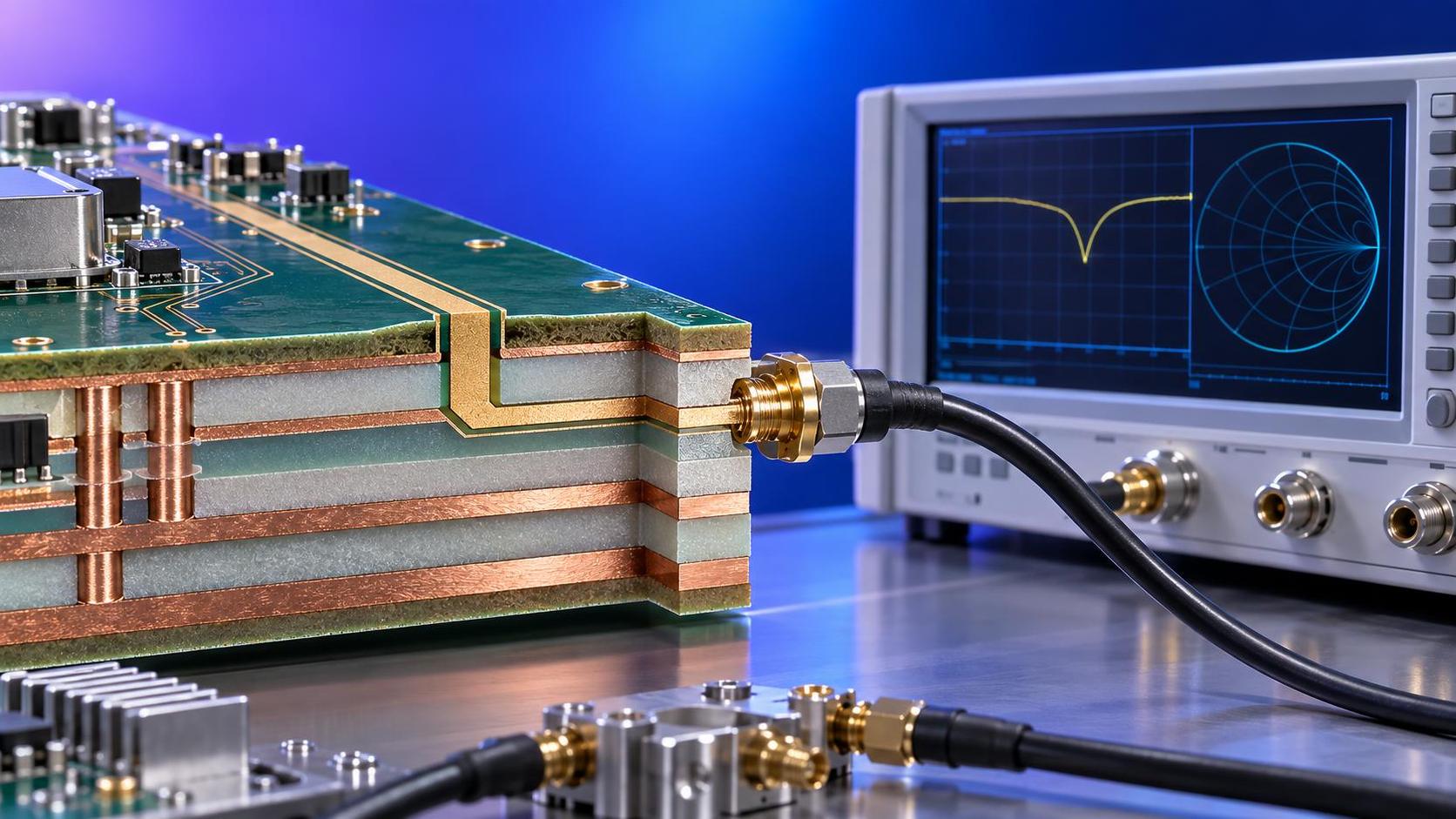
Then evaluate representative prototype panels using time-domain reflectometry, vector network analysis, and cross-sectional inspection. Test structures should match the real line types, lengths, and layer positions.
Compare measured impedance, phase delay, return loss, and insertion loss against predicted values. Significant differences should trigger model refinement or manufacturing process investigation before scaling production.
After qualification, maintain periodic monitoring through coupon testing and controlled material change management. Impedance stability is an ongoing production discipline, not a one-time engineering event.
Choosing the Right Dielectric Constant for RF Modules
There is no universally optimal dielectric constant for RF modules. The best choice depends on electrical architecture, available routing area, target impedance, loss requirements, cost constraints, and manufacturing maturity.
Lower-Dk materials can support faster signal propagation and reduced capacitive loading. They may be advantageous for high-frequency, low-loss, or phase-sensitive applications, but selection requires broader analysis.
Higher-Dk materials can reduce wavelength and enable more compact circuit structures. They may suit miniaturized filters, antennas, and resonators when their loss, tolerance, and temperature behavior remain acceptable.
For many evaluators, stable and well-characterized Dk is more valuable than an aggressively low nominal number. Predictability reduces rework, tuning effort, qualification risk, and field-performance uncertainty.
The ideal material also depends on the manufacturer’s demonstrated ability to process it. A premium laminate cannot deliver expected RF performance when lamination, etching, and impedance verification are poorly controlled.
Therefore, compare candidate materials using a combined scorecard: effective Dk stability, frequency behavior, loss, environmental performance, stackup compatibility, fabrication capability, and change-control quality.
Conclusion
Dielectric constant affects RF impedance stability because it controls electromagnetic propagation within the module stackup. Yet nominal Dk alone does not predict the performance of a finished product.
Technical evaluators should focus on effective Dk, frequency dependence, glass weave effects, resin distribution, copper roughness, geometric tolerance, and environmental stability when assessing RF material options.
The strongest qualification approach combines construction-specific modeling, production-representative testing, cross-sectional verification, and statistical process evidence. This converts material claims into defensible manufacturing confidence.
When selecting a dielectric constant for RF modules, prioritize repeatable electrical behavior over simplified datasheet comparisons. Stable impedance is ultimately achieved through controlled materials, controlled geometry, and controlled processes.
Recommended News
- RF ModulesHow dielectric constant affects impedance stability in RF modulesDielectric constant for RF modules directly affects impedance stability. Learn how Dk variation, stackup control, frequency, and fabrication impact RF performance.
- RF ModulesHow to Choose Low Power Wireless Modules for Battery-Driven DevicesWireless modules low power selection starts with real energy use, not datasheet claims. Learn how to compare RF, protocol fit, battery life, and reliability for smarter device design.
- RF ModulesEU WEEE Rule Takes Effect for Leaded RF ModulesEU WEEE rule now impacts leaded RF modules at import: Bluetooth and Wi-Fi shipments may be blocked without a Pb-exemption code. Learn key compliance steps to avoid customs delays.
- RF ModulesLow Power RF Transmitter Range Limits in Real DeploymentsLow power RF transmitter range depends on antennas, interference, enclosures, and regulations. Learn what really limits field performance and how to plan reliable deployment.
- RF ModulesRF Transmitter Price Breakdown: What Drives Total CostRF transmitter price depends on more than the quote. Discover how specs, certification, materials, and reliability testing shape total cost and smarter supplier decisions.
- RF ModulesVietnam to Require VCCI Pre-Approval for RF Module ImportsVietnam RF Module imports will require VCCI pre-approval from Aug 1, 2026. Learn how the new rule may affect customs clearance, supply chains, and sourcing plans.