
Do High-Performance Embedded Boards Need Different EMI Shielding?
DETAILS
The Short Answer: Usually Yes, but Not by Default
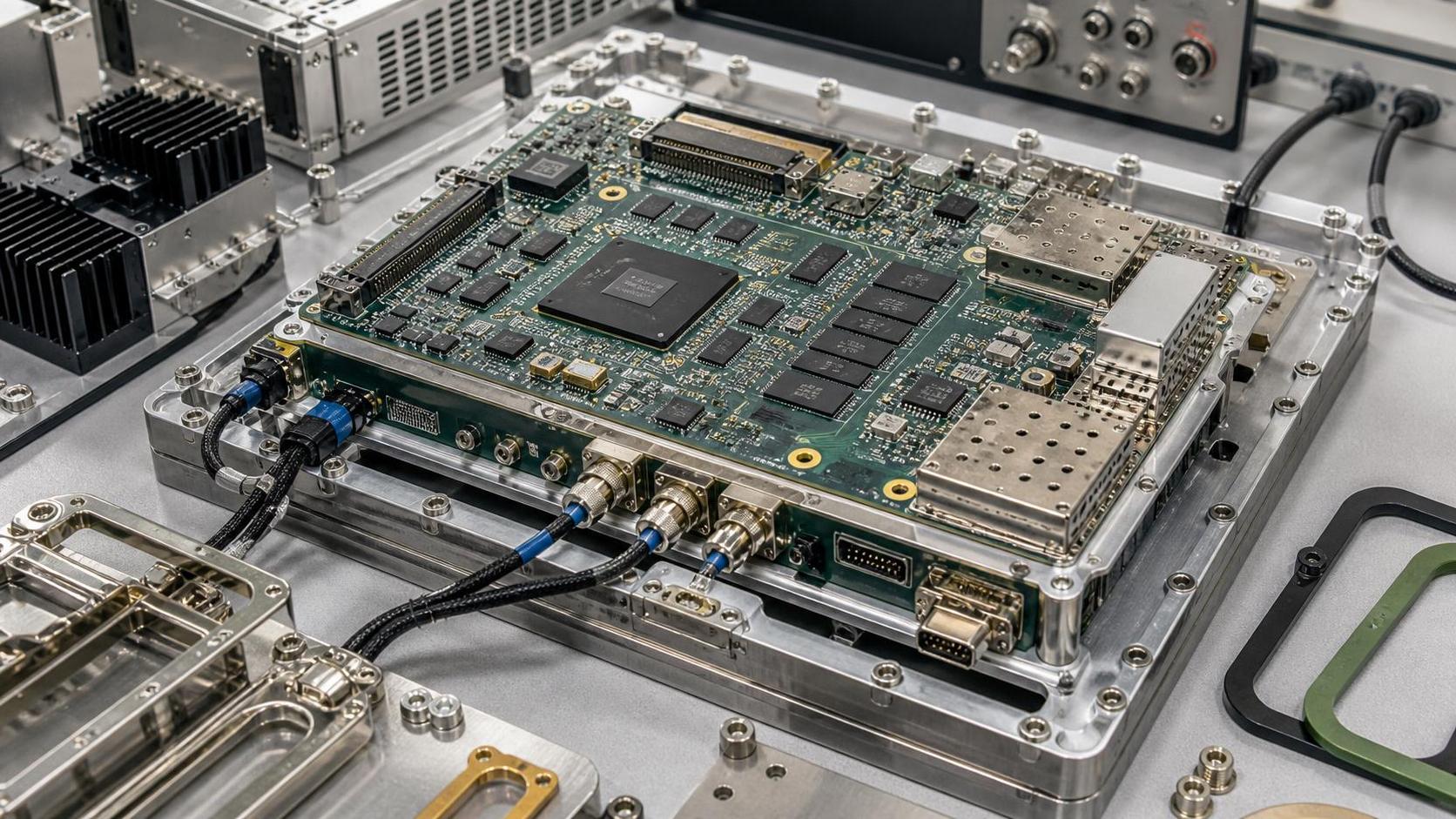
High-performance embedded boards often need a different EMI shielding approach, but the difference is not simply a matter of adding more metal, using a thicker gasket, or placing a shield can over the noisiest IC. The real change is that electromagnetic compatibility becomes a system-level design problem. As data rates rise, power conversion becomes denser, radio modules operate closer to digital logic, and thermal headroom narrows, shielding decisions interact directly with grounding, PCB stackup, enclosure design, cable routing, and manufacturing tolerances.
For a low-speed controller board in a spacious industrial enclosure, conventional shielding practices may be sufficient: a grounded metal enclosure, basic filtering at external interfaces, sensible trace routing, and reasonable separation between switching power stages and sensitive circuits. A compact embedded computing module, edge AI controller, automotive domain controller, medical imaging subassembly, or high-bandwidth communications board is different. It may combine fast serial interfaces, DDR memory, switching regulators, wireless radios, sensors, heat spreaders, and multiple external cables within a constrained mechanical envelope. In those conditions, EMI shielding is less an isolated component choice and more an architectural decision.
The practical question is not whether high-performance boards require shielding. Nearly all electronic systems need some level of electromagnetic control. The useful question is whether the existing shielding strategy still matches the board's frequency range, coupling paths, thermal requirements, assembly process, and compliance exposure.
Why High-Performance Boards Change the EMI Problem
Embedded systems create EMI through several mechanisms, including fast switching edges, clock harmonics, high-current power conversion, cable radiation, and unintended return-current paths. A board does not need to operate at an extremely high nominal frequency to generate emissions at much higher frequencies. Fast rise times in digital signals can produce broad harmonic content, while poorly controlled return paths can turn traces, connectors, seams, and cables into effective antennas.
In high-performance designs, these effects tend to compound. A processor may require multi-rail power delivery with high-current buck converters. Memory interfaces may run at frequencies where layout discontinuities become significant. High-speed links such as Ethernet, PCIe, USB, MIPI, LVDS, or proprietary serial interconnects may cross between board regions or leave the enclosure through connectors. At the same time, compact layouts reduce the distance between aggressors and victims.
That is why a shielding method that worked on an earlier-generation board can fail on a newer design even when the enclosure material and overall board dimensions appear similar. The source spectrum has changed, the geometry has changed, and the available paths for common-mode noise may have changed. A successful design must account for all three.
It is also important to distinguish between emissions control and immunity. A shield that helps prevent a system from radiating excessive noise may not, by itself, protect sensitive analog, RF, or safety-critical circuits from external interference. Procurement teams sometimes receive a shielding specification focused only on material attenuation or plating type, while engineering teams are concerned about enclosure seams, bonding continuity, cable penetration, and susceptibility under real operating conditions. Those are related issues, but they are not interchangeable.
When Conventional Shielding Stops Being Enough
Traditional approaches can remain effective when they are designed around the actual electromagnetic behavior of the product. The problem arises when teams treat shielding as a late-stage compliance remedy. A conductive enclosure added after layout, a generic EMI gasket selected by material data sheet, or a shield can placed over a processor may reduce one measurement while leaving the dominant coupling path untouched.
High-performance embedded boards typically warrant a more rigorous review when one or more of the following conditions are present:
- High-speed digital interfaces operate near switching power stages, RF circuits, or sensitive analog front ends.
- The design uses multiple cable assemblies, especially unshielded or long external cables that can carry common-mode currents.
- Thermal constraints require large openings, heat sinks, fans, thermal pads, or conductive chassis interfaces.
- The enclosure includes joints, doors, removable panels, coated surfaces, or dissimilar metals that may compromise electrical bonding.
- Component density has increased enough that physical separation is no longer a realistic noise-control method.
- The product will be used in electrically noisy environments such as factories, vehicles, telecom facilities, medical environments, or distributed energy systems.
- Compliance failure late in development would delay qualification, customer acceptance, or market entry.
None of these factors automatically mandates expensive shielding. They indicate that a simple material-based decision is unlikely to be sufficient. The team needs to identify dominant emissions sources and coupling routes before selecting the mitigation method.
Shielding Must Be Evaluated Alongside Grounding and Return Paths
The most common misunderstanding is that EMI shielding is primarily about blocking fields. In practical embedded systems, controlling return-current paths is often more important. A high-speed signal always needs a return path. When the intended path is interrupted by plane splits, connector transitions, poor chassis bonding, or poorly placed filtering, the current finds another route. That alternate route can increase radiated emissions, inject noise into nearby circuits, or create unexpected sensitivity to external fields.
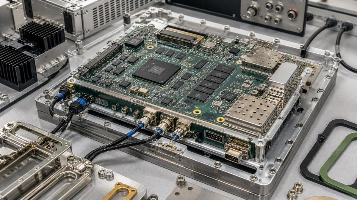
A metal enclosure can be highly conductive and still perform poorly if electrical continuity across seams is inconsistent. Similarly, a shield can over an RF or processor area may provide limited value if cable shields are terminated incorrectly or if external I/O allows noise to enter the system. A design should therefore examine the relationship among signal ground, chassis ground, cable shield termination, and enclosure bonding. There is no universal connection scheme that applies to every product. The right implementation depends on frequency, interface type, safety requirements, grounding environment, and enclosure architecture.
For instance, low-frequency grounding practice may encourage controlled separation between functional ground and chassis ground. At higher frequencies, long or inductive connections can become ineffective. A bonding strap, wire lead, or distant screw connection may look electrically connected in a DC continuity test while presenting substantial impedance at the frequencies that matter for emissions. This is one reason why mechanical design details, including screw spacing, contact area, plating, conductive gasketing, and paint removal at bond points, belong in the EMC discussion.
Board-Level, Compartment-Level, and Enclosure-Level Shielding Serve Different Purposes
Different shielding layers solve different problems. A disciplined design review should avoid selecting one layer as a substitute for another.
High-performance boards frequently need a coordinated combination of these layers. For example, a compact industrial gateway might use localized shields around a wireless module and switching regulator, internal partitions between compute and analog sensing regions, a conductive enclosure with controlled seams, and 360-degree cable-shield termination at selected external interfaces. The exact combination depends on the dominant noise path, not on a generic rule that more shielding always produces a better outcome.
Thermal Management Is Often the Constraint That Changes the Answer
High-performance embedded boards generate more heat, which makes EMI shielding more complicated. A shield can, heat spreader, enclosure wall, and thermal interface may all occupy the same physical space. Designers may need airflow openings, vent patterns, larger heat sinks, or thermally conductive pads that connect board-level components to the chassis. Each of these choices affects electromagnetic behavior.
Openings in a shielded enclosure are not automatically failures, but aperture size, shape, orientation, and placement matter. A vent pattern that is acceptable for one frequency range may be less effective as emissions move upward. Likewise, an exposed heat sink can become part of the radiating structure if it is coupled to a noisy source without a controlled return path. Thermal interface materials also vary in electrical conductivity. A material chosen solely for thermal performance may unintentionally alter grounding or isolation behavior.
There is a procurement implication here. Teams should not evaluate EMI gaskets, thermal pads, conductive foams, shield cans, and enclosure finishes as separate commodity line items when they function as part of a single electrical and mechanical system. Specifications should state the relevant operating temperature range, compression behavior, conductivity requirements, corrosion exposure, rework expectations, flame or environmental requirements where applicable, and acceptable manufacturing variation. A supplier's nominal data sheet values are useful, but finished-product performance depends heavily on assembly conditions.
Material Choice Matters, but It Is Not the First Decision
Conductive metals, plated plastics, conductive coatings, conductive fabrics, elastomer gaskets, metal mesh, and board-level shield frames all have roles in EMI control. Material selection should follow the definition of the problem rather than lead it. Teams sometimes overemphasize published shielding effectiveness values, which may have been measured under test conditions unlike the final product geometry.
A coating may offer a lighter or more flexible alternative to a metal enclosure, but its performance depends on thickness consistency, adhesion, grounding points, abrasion resistance, and the treatment of seams and openings. A conductive gasket may provide excellent contact when compressed correctly, yet underperform if fastener spacing is too wide, surfaces are painted, or repeated service cycles degrade compression. A plated enclosure may support robust conductivity but introduce corrosion or finish-control concerns in harsh environments.
For high-reliability systems, material qualification should include more than initial electrical measurements. Consider environmental cycling, vibration, humidity, salt exposure where relevant, mechanical service cycles, and changes in contact resistance over the expected product life. Requirements associated with IPC Class 3, ISO 9001-controlled production, customer-specific quality systems, or sector regulations should be interpreted as part of a broader validation plan, not as proof that a particular shielding architecture is suitable.
Do Not Trade EMI Compliance for Signal Integrity
Adding filters, ferrites, common-mode chokes, shield connections, or metal structures can solve one problem while creating another. High-speed serial channels have insertion-loss, impedance, skew, and return-loss budgets. A filter selected for noise suppression may degrade a link. A chassis bond or cable shield connection may alter common-mode behavior. A shield can placed too close to an RF antenna can detune it or reduce efficiency. A conductive thermal structure may introduce parasitic coupling near sensitive circuits.
This is why simulation, pre-compliance testing, and controlled prototype comparisons are particularly valuable for high-performance products. Full certification testing remains essential where required, but it is an expensive place to discover basic architecture problems. Early scans and near-field probing can help isolate whether emissions originate from a clock region, a power stage, a cable, a seam, or an interface transition. The goal is not to create a perfect laboratory model. It is to reduce uncertainty before the product reaches formal compliance testing and volume production.
What Sourcing and Engineering Teams Should Ask Before Locking the Design
For B2B buyers and engineering managers, a useful EMI shielding review should produce questions that suppliers can answer with evidence rather than broad claims.
- What is the suspected dominant noise source, and what evidence supports that conclusion?
- Which frequency bands and operating modes are most likely to create risk?
- Is the concern radiated emission, conducted emission, external immunity, internal interference, or a combination?
- How are cable shields, connector shells, chassis bonds, and PCB reference planes connected in the finished assembly?
- What happens to shielding and contact resistance after thermal cycling, vibration, corrosion exposure, or repeated service access?
- Does the shielding approach affect antenna performance, high-speed channel margins, thermal resistance, or assembly yield?
- Can the enclosure, gasket, coating, shield frame, and thermal interface be manufactured consistently across production sites?
- Which test data applies to the actual assembly, and which data applies only to a raw material or component coupon?
These questions are especially relevant when sourcing crosses regions or when design ownership, enclosure fabrication, PCB assembly, and final integration are handled by different suppliers. The failure mode is often not that one supplier delivered a defective part. It is that each supplier met its individual drawing while the combined system failed to maintain a continuous electromagnetic design intent.
Common Assumptions That Deserve Scrutiny
"A metal enclosure solves EMI." It can help substantially, but only when seams, openings, cables, grounding, and internal coupling are controlled. A conductive box with poor bonding or untreated interfaces may offer less real-world benefit than expected.
"Shielding effectiveness is a universal performance number." It is not. The measured result depends on frequency, test method, sample geometry, field type, contact condition, and installation. Use published values as comparative inputs, then validate the final design.
"More shielding is always safer." Additional shields can add thermal resistance, cost, weight, manufacturing complexity, access limitations, and signal-integrity risk. The right answer is targeted control of the dominant path.
"EMI issues can be fixed near the end." Some can. But late changes to enclosure tooling, PCB stackup, connector strategy, and thermal architecture are costly and disruptive. The earlier the coupling mechanism is understood, the more options remain available.
The Direction of Travel
The need for differentiated EMI shielding is likely to grow as embedded systems consolidate more functions into smaller devices. Higher compute density, faster interfaces, wider use of wireless connectivity, electrified equipment, distributed sensing, and tighter enclosure packaging all increase the chance that electromagnetic, thermal, and mechanical constraints collide.
For decision-makers, the useful response is not to standardize on the most aggressive shielding package. It is to make EMC a shared design input across PCB engineering, mechanical engineering, thermal design, manufacturing, and sourcing. High-performance embedded boards do require different approaches when their operating conditions and integration density demand it. The difference is less about a single exotic material than about treating shielding as part of the product architecture from the beginning.
Recommended News
- EMI ShieldingHow to choose a design verification resource for EMI testingDesign verification resource guide for EMI testing: compare technical depth, traceable evidence, and compliance insight to prevent costly redesigns.
- EMI ShieldingHow automotive component compliance testing supports EMC approvalComponent compliance testing automotive helps secure EMC approval through traceability, pre-compliance checks, and controlled design changes. Learn how to reduce risk.
- EMI ShieldingDo High-Performance Embedded Boards Need Different EMI Shielding?Do high-performance embedded boards require different EMI shielding approaches? Explore practical strategies for grounding, thermal design, cable control, compliance, and reliable performance.
- EMI ShieldingEU Adds Halogenated Flame Retardants and EMI Coatings to RoHS ScopeEU RoHS scope expands to halogenated flame retardants and EMI coatings under Directive (EU) 2026/1389. See how PCB exporters can prepare for the 2027 compliance deadline.
- EMI ShieldingEU Requires EPDs for EMI Shielding PartsEU Requires EPDs for EMI Shielding Parts from January 2027. Learn how the new EU rule affects compliance, carbon disclosure, shipment timing, and supplier planning.
- EMI ShieldingCBP Tightens Filing Rules for EMI Shielding ImportsCBP Tightens Filing Rules for EMI Shielding Imports: learn how the September 2026 ACE filing change affects RoHS, REACH, customs timing, and buyer risk for U.S.-bound shipments.